




A research team at ETH Zurich has announced the development of a revolutionary optical component known as the "Fourier pixel," a technological breakthrough that merges the functions of light emission and light detection into a single microscopic unit. Published in the journal Nature in mid-2026, the study details a paradigm shift in how digital displays and camera sensors are engineered. For decades, the hardware responsible for showing an image (displays) and the hardware responsible for capturing one (sensors) have remained physically distinct entities. The Fourier pixel eliminates this boundary, utilizing the principles of wave interference and nanostructured surfaces to control and analyze light waves simultaneously.
This innovation, led by materials engineer David Norris and postdoctoral researcher Sander Vonk, represents a significant leap in nanophotonics. By carving intricate, wave-shaped patterns into a chip’s surface, the researchers have created a medium where light does not simply bounce off a surface or pass through a filter, but is instead "sculpted" at the level of individual waves. This allows a single pixel to act as both a source of steered light and a sensor capable of decomposing incoming light into its constituent properties, including amplitude, phase, and polarization.
The Physics of Interference and the Fourier Principle
At the core of the Fourier pixel is the fundamental physical phenomenon of interference. In classical optics, when light waves encounter a surface, they scatter. If multiple waves overlap, they can undergo constructive interference—where the peaks of the waves align to create a stronger signal—or destructive interference, where the waves cancel each other out. Traditional pixels in an LED or OLED screen rely on the intensity of light emitted by sub-pixels (typically red, green, and blue). In contrast, the Fourier pixel uses a "sculpted" surface profile to manipulate the very phase of the light.
The technology derives its name from Fourier analysis, a mathematical method developed by Joseph Fourier in the early 19th century. Fourier analysis allows complex signals to be broken down into a series of simpler sine waves. In the context of these new pixels, the researchers used Fourier transforms to calculate the exact surface geometry required to produce specific optical effects. By mathematically determining the necessary surface profile, the team can program a pixel to turn an incoming light wave into a "surface wave" that travels across the chip. This wave is then scattered back out at a different point within the same pixel, creating a controlled light output.
Because the process is reversible, the same structure used to emit a specific light pattern can also be used to analyze incoming light. When external light hits the patterned pixel, the resulting surface waves carry information about the light’s origin, color, and polarization. This data can be captured and processed, effectively turning the display into a high-resolution camera.
Chronology of Development and the "ETH" Proof of Concept
The journey toward the Fourier pixel began with theoretical models of metasurfaces—engineered materials with properties not found in nature. Over the past decade, researchers have experimented with "flat optics," attempting to replace bulky glass lenses with nanostructured surfaces. The ETH Zurich team sought to take this a step further by making these surfaces multifunctional.
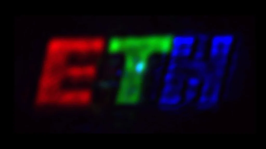
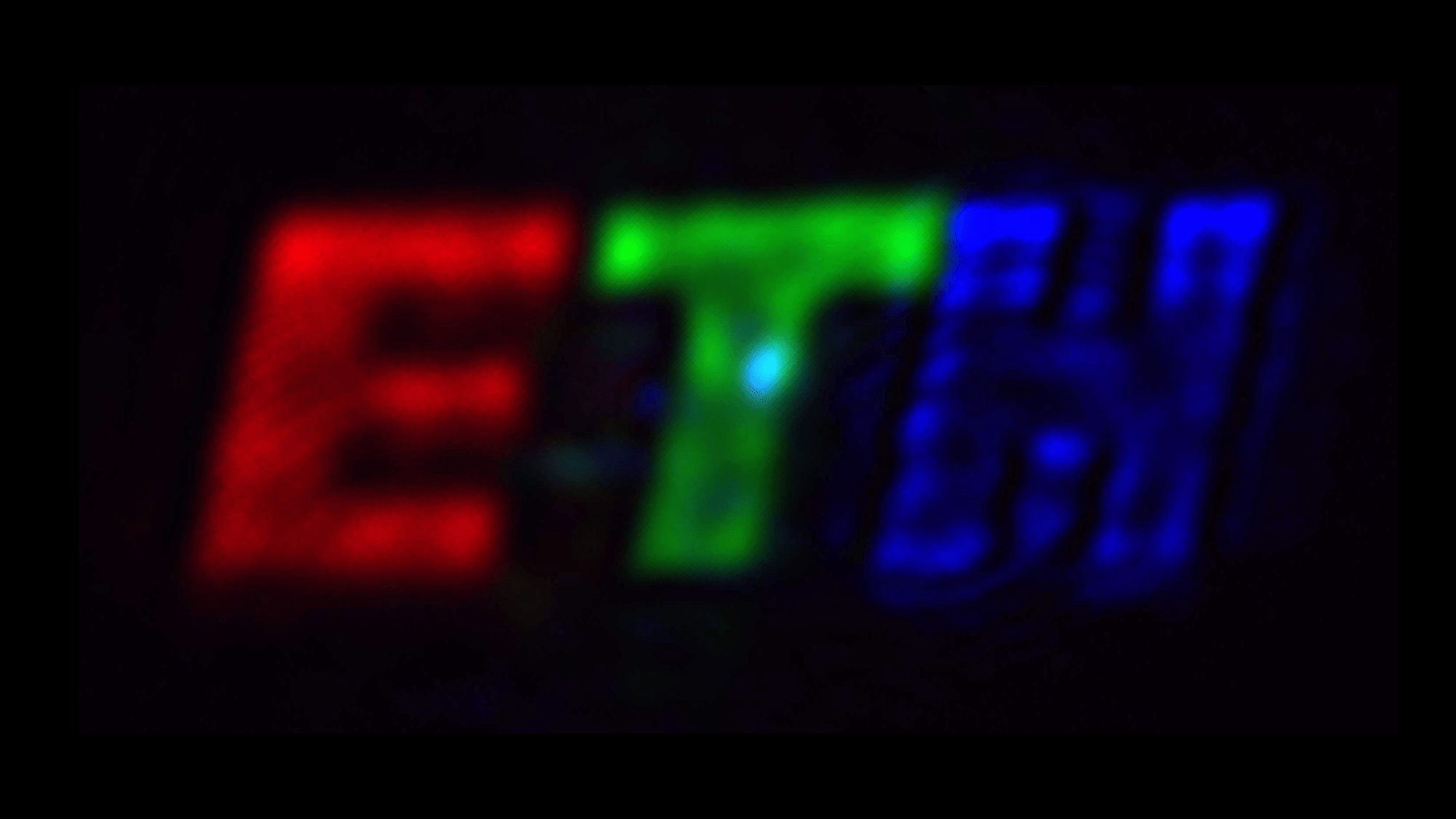
In early 2025, the team began perfecting the lithography techniques required to carve patterns at the nanometer scale with enough precision to handle visible light spectra. By the beginning of 2026, they had successfully produced a prototype chip. To demonstrate the capability of the technology, the researchers created a microscopic version of the ETH Zurich university logo using a matrix of Fourier pixels. The "E" was rendered in red, the "T" in green, and the "H" in blue. Unlike traditional displays that use color filters, these colors were generated through the precise geometric scattering of light, ensuring higher purity and lower energy loss.
The results, published in Nature under the title "Multifunctional Fourier Pixels for Light Control and Analysis," confirm that these pixels can be manufactured using existing semiconductor fabrication processes, albeit with higher precision requirements than standard consumer-grade chips.
Technical Specifications and Comparative Data
The Fourier pixel offers several advantages over the traditional CMOS (Complementary Metal-Oxide-Semiconductor) sensors found in modern smartphones and the OLED (Organic Light Emitting Diode) pixels found in high-end televisions.
- Spatial Efficiency: In a standard smartphone, the camera is a separate module that requires a "notch" or a hole-punch cutout in the screen. Under-display cameras exist but often suffer from poor image quality because light must struggle through the display layers. Fourier pixels solve this by making the display itself the camera.
- Phase and Polarization Sensing: Standard cameras only capture light intensity (how bright it is) and color. Fourier pixels can detect the "phase" of light (the position of the wave in its cycle) and its polarization (the direction in which the wave vibrates). This is critical for applications like facial recognition, 3D mapping, and medical imaging.
- Computational Reduction: Traditional image processing requires a powerful CPU or GPU to interpret raw data from a sensor. Because the Fourier pixel performs a physical version of a Fourier transform, much of the "math" of image processing happens at the hardware level before the data even reaches a processor.
According to the study, the Fourier pixel matrix demonstrated a 30% increase in light-coupling efficiency compared to traditional metasurface emitters. Furthermore, the ability to control light polarization at the pixel level could lead to displays that are perfectly visible even in direct sunlight or through polarized sunglasses without the loss of brightness associated with current filters.
Official Responses and Scientific Impact
The scientific community has reacted with cautious optimism toward the findings. Sander Vonk emphasized the simplicity of the mathematical approach, noting that because the surface profiles are determined through Fourier analysis, the design process does not require the massive computational power typically associated with simulating complex optical environments. "We can combine the control and analysis of amplitude, phase, and polarization on a single pixel," Vonk stated, highlighting the versatility of the design.
David Norris, the study’s co-author, pointed toward the broader implications for materials science. "Our new pixels for control and analysis could, therefore, become a useful tool in many areas," Norris said. He suggested that the immediate goal for the team is to move beyond static logos and create a dynamic "matrix" or "active-matrix" of pixels that can change their properties in real-time, similar to how pixels on a computer screen refresh 60 or 120 times per second.
Industry analysts suggest that if the technology can be scaled, it would disrupt the multi-billion dollar display and sensor markets currently dominated by firms in South Korea, Japan, and Taiwan. However, experts note that the transition from a laboratory "proof of concept" to mass-produced consumer electronics typically takes five to ten years.
Broader Implications and Future Applications
The potential applications for Fourier pixels extend far beyond consumer electronics. In the field of autonomous vehicles, for instance, the ability for a single surface to both project LiDAR pulses and analyze their return could lead to more aerodynamic and integrated sensor suites. Currently, self-driving cars rely on bulky, rotating sensor domes; Fourier pixel "skins" could allow the entire body of a car to act as a 360-degree vision system.
In medical technology, Fourier pixels could revolutionize endoscopy and microscopy. A single, flat chip could serve as a high-resolution microscope that doesn’t require complex lens assemblies, making diagnostic tools smaller, cheaper, and more portable. Furthermore, the polarization-sensing capabilities of these pixels could be used to detect specific biological tissues or chemical compounds that are invisible to standard cameras.
For the average consumer, the most immediate impact might be the "invisible" camera. Future laptops, tablets, and phones could feature screens that capture a user’s image from every point on the display, allowing for perfect eye contact during video calls—a feat currently impossible because cameras are located at the top of the screen.
The ETH Zurich team is now focusing on "dynamic" Fourier pixels. The current prototype uses a fixed, carved pattern. The next generation of research aims to incorporate materials that can change their shape or refractive index in response to an electrical signal. If successful, this would allow a single screen to toggle between being a high-definition movie display, a 3D scanner, and a biometric fingerprint reader across its entire surface.
As the tech industry moves toward the "post-smartphone" era of augmented reality (AR) and wearable tech, the Fourier pixel provides a necessary hardware foundation. By shrinking the footprint of optical systems while expanding their functionality, the researchers at ETH Zurich have paved the way for a future where the line between the digital and physical worlds is thinner than a wavelength of light.